Continuing from the last time , I will take a look at the TRD of the zcu106 PCI Express. First, let’s examine the PCI Express standard. However, the standard is not available on the internet, so check it from wikipedia.
https://ja.wikipedia.org/wiki/PCI_Express
First check the physical wiring.
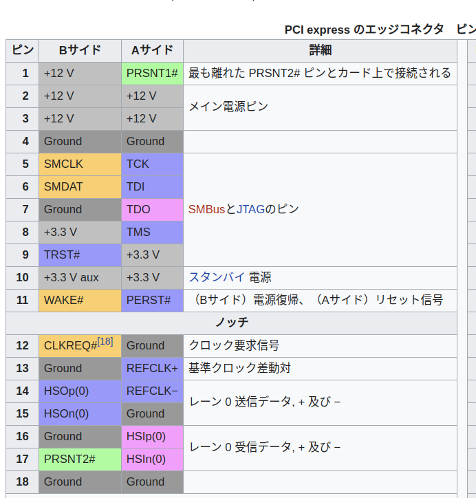
magine each PIN. Write the explanation with the image seen from the RC side (for example, the PC side).
| PIN | Side | Name | |
| 1 | A | PRSNT1 # | PIN to check if Card is connected |
| 1 | B | +12V | Power supply |
| Four | A | Ground | ground |
| Five | A | TCK | For JTAG |
| Five | B | SMCLK | SM Bus. Maybe for auxiliary communication |
| 6 | A | TDI | For JTAG |
| 6 | B | SMDAT | SM Bus. Maybe for auxiliary communication |
| 7 | A | TDO | For JTAG |
| 8 | A | ETC | SM Bus. Maybe for auxiliary communication |
| 8 | B | + 3.3V | Power supply |
| 9 | B | TRIESTE # | For JTAG |
| Ten | B | + 3.3V to | Power supply for aux. |
| 11 | A | PRESS # | reset. A signal that the RC side resets the card. |
| 11 | B | WAKE # | Power return. Notify you that you have returned when you save power? |
| 12 | B | CLKREQ# | Clock request. Is it time for the card to request a clock? |
| 13 | A | REFCLK+ | Reference clock differential +. |
| 14 | A | REFCLK- | Reference clock differential. |
| 14 | B | HSOp(0) | Lane 0 transmission. Differential +. |
| 15 | B | HSOn(0) | Lane 0 transmission. Differential. |
| 16 | A | HSlp(0) | Lane 0 reception. Differential + |
| 17 | A | HSln (0) | Lane 0 reception. Differential. |
I took a look up to x1. The number of lanes will increase to x4 and x16, but basically, only the signals of PRST and lane will be added.
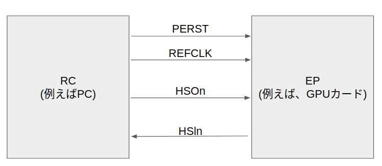
I think REFCLK, HSOp, HSlp, and PERST are important signals, except for the auxiliary and power save.
Excluding the power supply, I think it is logically the following block diagram.